- 您现在的位置:买卖IC网 > Sheet目录2003 > LTC1279CG#TRPBF (Linear Technology)IC A/DCONV SAMPLNG W/SHTDN24SSOP
8
LTC1279
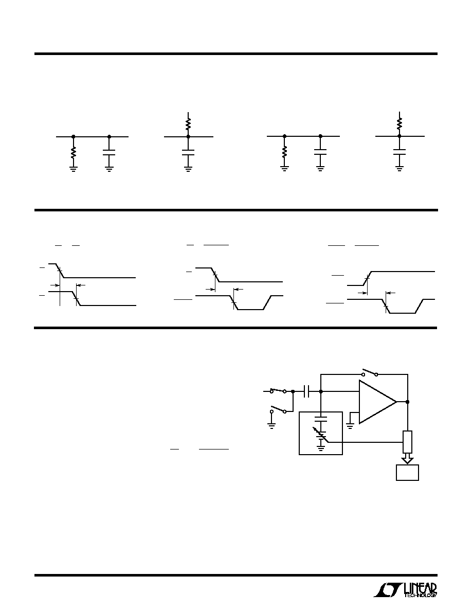
TEST CIRCUITS
Load Circuits for Output Float Delay
Load Circuits for Access Timing
3k
CL
DBN
DGND
A) HIGH-Z TO VOH (t8)
AND VOL TO VOH (t6)
CL
DBN
3k
5V
B) HIGH-Z TO VOL (t8)
AND VOH TO VOL (t6)
DGND
1279 TC01
3k
10pF
DBN
DGND
A) VOH TO HIGH-Z
10pF
DBN
3k
5V
B) VOL TO HIGH-Z
DGND
1279 TC02
CS to RD Setup Timing
SHDN to CONVST Wake-Up Timing
CS to CONVST Setup Timing
TI I G DIAGRA S
WU
W
APPLICATIONS INFORMATION
WU
U
CONVERSION DETAILS
The LTC1279 uses a successive approximation algorithm
and an internal sample-and-hold circuit to convert an
analog signal to a 12-bit parallel output. The ADC is
complete with a precision reference and an internal clock.
The control logic provides easy interface to microproces-
sors and DSPs. (Please refer to the Digital Interface
section for the data format.)
Conversion start is controlled by the CS and CONVST
inputs. At the start of conversion the successive approxi-
mation register (SAR) is reset. Once a conversion cycle
has begun it cannot be restarted.
During conversion, the internal 12-bit capacitive DAC
output is sequenced by the SAR from the most significant
bit (MSB) to the least significant bit (LSB). Referring to
Figure 1, the AIN input connects to the sample-and-hold
capacitor during the acquire phase, and the comparator
offset is nulled by the feedback switch. In this acquire
phase, a minimum delay of 160ns will provide enough
VDAC
1279 F01
+
–
CDAC
DAC
SAMPLE
HOLD
CSAMPLE
S
A
R
12-BIT
LATCH
COMPAR-
ATOR
SAMPLE
SI
AIN
Figure 1. AIN Input
t3
SHDN
CONVST
1279 TD03
t1
CS
RD
1279 TD01
t2
CS
CONVST
1279 TD02
time for the sample-and-hold capacitor to acquire the
analog signal. During the convert phase, the comparator
feedback switch opens, putting the comparator into the
compare mode. The input switch switches CSAMPLE to
ground, injecting the analog input charge onto the sum-
ming junction. This input charge is successively com-
发布紧急采购,3分钟左右您将得到回复。
相关PDF资料
LTC1282ACN#PBF
IC A/D CONV SAMPLING W/REF 24DIP
LTC1288IS8#TRPBF
IC A/D CONV SAMPLING 12BIT 8SOIC
LTC1298IS8#TRPBF
IC A/D CONV SAMPLING 12BIT 8SOIC
LTC1327CNW#PBF
IC TXRX EIA/TIA-562 3.3V 28-DIP
LTC1329ACS8-50#TRPBF
IC D/A CONV 8BIT MICROPWR 8-SOIC
LTC1337CNW#PBF
IC 3DVR/5RCVR 5V RS232 28-DIP
LTC1382IN#PBF
IC TXRX 5V RS232 W/SHTDWN 18-DIP
LTC1383IS#TRPBF
IC TXRX 5V RS232 LOW PWR 16-SOIC
相关代理商/技术参数
LTC1279CSW
功能描述:IC A/DCONV SAMPLNG W/SHTDN24SOIC RoHS:否 类别:集成电路 (IC) >> 数据采集 - 模数转换器 系列:- 标准包装:1,000 系列:- 位数:12 采样率(每秒):300k 数据接口:并联 转换器数目:1 功率耗散(最大):75mW 电压电源:单电源 工作温度:0°C ~ 70°C 安装类型:表面贴装 封装/外壳:24-SOIC(0.295",7.50mm 宽) 供应商设备封装:24-SOIC 包装:带卷 (TR) 输入数目和类型:1 个单端,单极;1 个单端,双极
LTC1279CSW#PBF
功能描述:IC A/DCONV SAMPLNG W/SHTDN24SOIC RoHS:是 类别:集成电路 (IC) >> 数据采集 - 模数转换器 系列:- 其它有关文件:TSA1204 View All Specifications 标准包装:1 系列:- 位数:12 采样率(每秒):20M 数据接口:并联 转换器数目:2 功率耗散(最大):155mW 电压电源:模拟和数字 工作温度:-40°C ~ 85°C 安装类型:表面贴装 封装/外壳:48-TQFP 供应商设备封装:48-TQFP(7x7) 包装:Digi-Reel® 输入数目和类型:4 个单端,单极;2 个差分,单极 产品目录页面:1156 (CN2011-ZH PDF) 其它名称:497-5435-6
LTC1279CSW#TR
功能描述:IC ADC 12BIT SAMPL SHTDWN 24SOIC RoHS:否 类别:集成电路 (IC) >> 数据采集 - 模数转换器 系列:- 标准包装:1,000 系列:- 位数:12 采样率(每秒):300k 数据接口:并联 转换器数目:1 功率耗散(最大):75mW 电压电源:单电源 工作温度:0°C ~ 70°C 安装类型:表面贴装 封装/外壳:24-SOIC(0.295",7.50mm 宽) 供应商设备封装:24-SOIC 包装:带卷 (TR) 输入数目和类型:1 个单端,单极;1 个单端,双极
LTC1279CSW#TRPBF
功能描述:IC A/DCONV SAMPLNG W/SHTDN24SOIC RoHS:是 类别:集成电路 (IC) >> 数据采集 - 模数转换器 系列:- 标准包装:1,000 系列:- 位数:12 采样率(每秒):300k 数据接口:并联 转换器数目:1 功率耗散(最大):75mW 电压电源:单电源 工作温度:0°C ~ 70°C 安装类型:表面贴装 封装/外壳:24-SOIC(0.295",7.50mm 宽) 供应商设备封装:24-SOIC 包装:带卷 (TR) 输入数目和类型:1 个单端,单极;1 个单端,双极
LTC1279CSWPBF
制造商:Linear Technology 功能描述:LTC1279CSWPBF
LTC1279IG
功能描述:IC A/DCONV SAMPLNG W/SHTDN24SSOP RoHS:否 类别:集成电路 (IC) >> 数据采集 - 模数转换器 系列:- 标准包装:1,000 系列:- 位数:12 采样率(每秒):300k 数据接口:并联 转换器数目:1 功率耗散(最大):75mW 电压电源:单电源 工作温度:0°C ~ 70°C 安装类型:表面贴装 封装/外壳:24-SOIC(0.295",7.50mm 宽) 供应商设备封装:24-SOIC 包装:带卷 (TR) 输入数目和类型:1 个单端,单极;1 个单端,双极
LTC1279IG#PBF
功能描述:IC A/DCONV SAMPLNG W/SHTDN24SSOP RoHS:是 类别:集成电路 (IC) >> 数据采集 - 模数转换器 系列:- 标准包装:1,000 系列:- 位数:12 采样率(每秒):300k 数据接口:并联 转换器数目:1 功率耗散(最大):75mW 电压电源:单电源 工作温度:0°C ~ 70°C 安装类型:表面贴装 封装/外壳:24-SOIC(0.295",7.50mm 宽) 供应商设备封装:24-SOIC 包装:带卷 (TR) 输入数目和类型:1 个单端,单极;1 个单端,双极
LTC1279IG#TR
功能描述:IC ADC 12BIT SAMPL SHTDWN 24SSOP RoHS:否 类别:集成电路 (IC) >> 数据采集 - 模数转换器 系列:- 标准包装:1,000 系列:- 位数:12 采样率(每秒):300k 数据接口:并联 转换器数目:1 功率耗散(最大):75mW 电压电源:单电源 工作温度:0°C ~ 70°C 安装类型:表面贴装 封装/外壳:24-SOIC(0.295",7.50mm 宽) 供应商设备封装:24-SOIC 包装:带卷 (TR) 输入数目和类型:1 个单端,单极;1 个单端,双极